Chemical-mechanical planarization (CMP) is a vital process in semiconductor manufacturing. It plays a significant role in ensuring that wafer surfaces are smooth and uniform, which is essential for the performance of integrated circuits.
This article delves deeply into the CMP process, its mechanisms, components, advantages, challenges, and innovations, providing a complete picture of its significance in the semiconductor industry.
What is CMP?
CMP is a process that smooths the surface of a semiconductor wafer by using a combination of chemical reactions and mechanical polishing. The main goal is to remove any topographical variations on the wafer surface.
These variations can occur during previous fabrication steps, such as etching or deposition. The CMP process ensures a uniform surface, which is crucial for subsequent layers of materials.
The Mechanisms Behind CMP
CMP operates on two key principles:
Chemical Reaction:
The use of chemically reactive slurries allows for selective removal of material. Chemical agents in the slurry can react with specific materials to facilitate easier removal.
Mechanical Abrasion:
The mechanical aspect involves physical polishing, where the abrasive particles in the slurry work against the wafer surface to remove material and achieve a flat finish.
Together, these mechanisms enable CMP to effectively achieve the required surface quality.
Key Components of CMP
The CMP process consists of several critical components that work in unison to achieve the desired results:
Polishing Pad
The polishing pad is typically made from soft, porous materials such as polyurethane. It serves as the contact surface between the wafer and the polishing equipment. The pad is designed to absorb the slurry and maintain consistent pressure during polishing.
Slurry
Slurry is a mixture of abrasive particles suspended in a liquid medium. The composition of the slurry varies based on the material being polished. For instance, silica-based slurries are commonly used for silicon dioxide, while copper slurries contain different chemical additives.
Wafer Carrier
The wafer carrier holds the wafer in place during the CMP process. It applies pressure to ensure that the wafer maintains contact with the polishing pad while rotating.
CMP Equipment
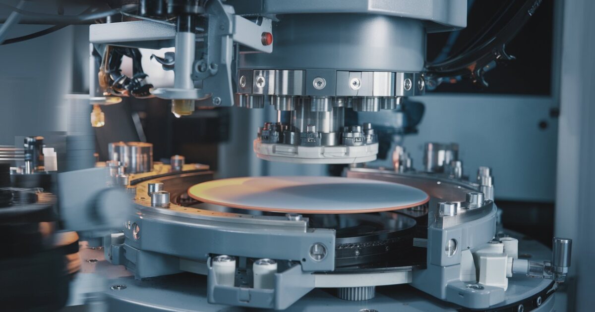
Specialized equipment is used for CMP, including a rotating platen where the polishing pad is mounted. The system often incorporates features for controlling the speed, pressure, and slurry distribution.
CMP Process Steps
The CMP process consists of several distinct steps that ensure effective wafer polishing:
- Wafer Preparation: The wafer is cleaned to remove any contaminants that may interfere with the polishing process. This step is crucial to avoid introducing defects during CMP.
- Slurry Application: A suitable slurry is applied to the polishing pad. The slurry’s composition is carefully chosen based on the type of material being polished.
- Polishing: The wafer is placed on the polishing pad, which is rotated. The mechanical force combined with the chemical action of the slurry smooths the wafer surface. The process involves maintaining precise pressure and speed to achieve optimal results.
- Post-Polishing Cleaning: Once polishing is complete, the wafer undergoes a thorough cleaning to remove any residual slurry and particles. This step is essential to ensure that the wafer is ready for subsequent fabrication steps.
- Inspection: After cleaning, the wafer is inspected for flatness and surface quality. Various metrology techniques are used to ensure it meets the required specifications.
Types of CMP Processes
CMP can be classified into several categories based on the materials being polished:
Oxide CMP
This process typically involves polishing silicon dioxide layers. It is crucial for achieving planarization in multi-layer devices.
Metal CMP
Used primarily for polishing metal interconnects like copper, metal CMP processes utilize different slurries that enhance the removal rate while minimizing defects.
Dielectric CMP
This type involves polishing low-k dielectrics, which are critical for reducing capacitance and improving performance in advanced semiconductor devices.
SiGe and SiC CMP
Specific processes are developed for polishing silicon-germanium (SiGe) and silicon carbide (SiC) materials, which are used in specialized applications.
Advantages of CMP
CMP offers numerous benefits in semiconductor manufacturing:
| Benefits | Description |
|---|---|
| High Surface Quality | CMP achieves superior flatness, essential for the performance of multilayered semiconductor devices. |
| Defect Reduction | A smoother surface from CMP reduces defects, enhancing device yield and overall performance. |
| Process Versatility | CMP can be applied to a range of materials, including oxides, metals, and dielectrics, providing flexibility for different semiconductor processes. |
Challenges in CMP
Despite its advantages, CMP comes with several challenges that manufacturers must address:
Defect Control:
The risk of introducing defects during the CMP process is significant. Controlling defects such as scratches and pits is crucial to maintaining device quality.
Material Removal Rate (MRR):
Achieving the optimal MRR is essential for efficient production. A high MRR may lead to wafer damage, while a low MRR can slow down the manufacturing process.
Slurry Management:
The composition and quality of the slurry must be carefully monitored. Variations in slurry quality can lead to inconsistent polishing results.
Equipment Complexity:
CMP equipment is sophisticated and requires regular maintenance and calibration to ensure precise operation.
Innovations and Future Trends in CMP
The semiconductor industry is continuously evolving, and so is CMP technology. Key innovations and trends include:
Advanced Slurries
Researchers are developing new slurries that enhance the removal rate while minimizing defects. These advanced formulations aim to improve efficiency and effectiveness in CMP.
Automation and Control
Increasing automation in CMP processes allows for better precision and control. Advanced sensors and control systems can optimize polishing parameters in real time.
Eco-Friendly Practices
There is a growing focus on sustainability in semiconductor manufacturing. Efforts are being made to develop environmentally friendly slurries and minimize waste in the CMP process.
Nanotechnology
The integration of nanotechnology in CMP is gaining attention. Nanoparticles can be used to enhance the polishing process and achieve superior surface finishes.
Conclusion
Chemical-mechanical planarization is an essential process in semiconductor manufacturing, ensuring the quality and reliability of electronic devices. By combining chemical reactions with mechanical polishing, CMP achieves the desired surface flatness required for advanced technologies. Despite the challenges it presents, ongoing innovations are shaping the future of CMP, making it more efficient and environmentally friendly.
Understanding CMP’s intricacies and advancements helps appreciate its crucial role in the semiconductor industry. As technology continues to progress, CMP will remain a cornerstone of semiconductor manufacturing, enabling the production of faster, smaller, and more efficient electronic devices that drive our modern world.
FAQ’s
What is chemical mechanical planarization used for?
Chemical mechanical planarization (CMP) is used to smooth and flatten the surface of semiconductor wafers. This process removes uneven layers, allowing for precise layering of materials, which is essential for creating reliable and high-performance microchips and electronic devices.
What is the CMP technique?
The CMP technique is a process that combines chemical and mechanical actions to polish semiconductor wafers. It involves applying a slurry containing abrasives and chemicals to the wafer surface while using a rotating polishing pad. This technique effectively removes material, achieving a smooth and flat surface essential for multi-layer semiconductor devices.
What is the difference between lapping and CMP?
Lapping uses mechanical grinding to flatten surfaces, while CMP combines chemical and mechanical processes for smoother, defect-free results. CMP is preferred for precise semiconductor manufacturing.
What is the chemical mechanical polishing mechanism?
The chemical-mechanical polishing (CMP) mechanism uses a slurry containing abrasive particles and chemicals. The slurry chemically softens the surface, while mechanical abrasion from the pad removes material, creating a smooth, flat surface.
What is CMP process in VLSI?
In VLSI (Very Large Scale Integration), the CMP process involves polishing semiconductor wafers to achieve a flat and smooth surface. This is crucial for multi-layer fabrication, as it ensures proper layer alignment and improves the performance and yield of integrated circuits.
